Thin Film Deposition Techniques Transforming Modern Electronics
Thin Film Deposition Processes Simplified for Beginners
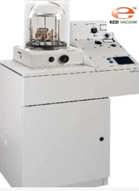
Basic Information
In the fast-paced world of electronics, innovation is often measured in nanometers. Devices have become smaller, faster, and more efficient, thanks to advancements in material science. Among these breakthroughs, thin film deposition has emerged as a cornerstone technology, enabling the creation of ultra-precise layers of materials that define the performance of modern electronic devices.
Understanding Thin Film Deposition
At its core, thin film deposition refers to the process of depositing extremely thin layers of materials—ranging from a few nanometers to several micrometers—onto a substrate. These layers are crucial for manufacturing semiconductors, solar cells, optical coatings, and other high-tech components. By controlling the thickness, composition, and uniformity of these films, engineers can manipulate electrical, optical, and mechanical properties to achieve the desired functionality.
There are two primary categories of thin film deposition techniques: physical vapor deposition (PVD) and chemical vapor deposition (CVD). Each method offers unique advantages and is selected based on the specific application requirements.
Physical Vapor Deposition (PVD)
PVD involves physically transferring material from a source to the substrate. Techniques under PVD include thermal evaporation, sputtering, and molecular beam epitaxy.
-
Thermal Evaporation: In this method, the material is heated until it vaporizes and then condenses on the substrate, forming a thin film. It is widely used for metallic coatings and reflective surfaces.
-
Sputtering: Here, energetic particles bombard a target material, causing atoms to be ejected and deposited onto the substrate. This approach is particularly useful for creating uniform films on large surfaces.
-
Molecular Beam Epitaxy (MBE): MBE is a highly controlled process used in semiconductor fabrication. It allows precise layering at the atomic level, essential for modern microelectronics.
The success of PVD techniques heavily depends on maintaining a clean, controlled environment. This is where a scientific vacuum pump becomes indispensable, creating the low-pressure conditions necessary to prevent contamination and ensure consistent film quality.
Chemical Vapor Deposition (CVD)
Unlike PVD, CVD relies on chemical reactions to produce thin films. Precursors in gaseous form react or decompose on the heated substrate surface, forming a solid layer. Variants of CVD include plasma-enhanced CVD (PECVD), low-pressure CVD (LPCVD), and atomic layer deposition (ALD).
-
Plasma-Enhanced CVD: By using plasma to initiate chemical reactions, PECVD allows deposition at lower temperatures, which is crucial for heat-sensitive substrates.
-
Atomic Layer Deposition: ALD is a technique that builds films one atomic layer at a time, offering unmatched precision and uniformity. It has become vital in producing high-performance microchips and memory devices.
The efficiency of CVD processes is also augmented by vacuum technology, with a scientific vacuum pump ensuring the required environment for controlled reactions and minimizing impurities.
Applications Driving Modern Electronics
The impact of thin film deposition spans multiple sectors of electronics:
-
Semiconductors: High-performance processors and memory chips rely on thin films for transistor gates, interconnects, and insulation layers.
-
Optoelectronics: Devices such as LEDs, photodetectors, and laser diodes require thin films for enhanced light absorption and emission properties.
-
Solar Technology: Thin film solar cells utilize specialized coatings to improve energy conversion efficiency and reduce material costs.
-
Flexible Electronics: Wearable devices and foldable screens employ thin films for transparent conductive layers and encapsulation.
Each of these applications demands precision and reliability, reinforcing the importance of advanced deposition methods and high-quality vacuum systems.
Advancements Enhancing Film Quality
Modern innovations in thin film deposition are focused on increasing efficiency, scalability, and environmental sustainability. Techniques like atomic layer deposition now allow atomic-level precision, while newer scientific vacuum pump designs offer superior control, reduced energy consumption, and longer operational life. Furthermore, the integration of in-situ monitoring tools enables real-time adjustments during deposition, ensuring consistent film thickness and composition.
Challenges and Future Prospects
Despite its advantages, thin film deposition faces several challenges. Controlling defects at the nanoscale, achieving uniform deposition on large substrates, and reducing manufacturing costs remain key areas of research. Emerging trends include hybrid deposition techniques that combine the strengths of PVD and CVD and the development of eco-friendly processes that minimize hazardous chemicals.
As electronics continue to shrink and performance demands grow, thin film deposition will remain a critical technology. Advances in deposition methods and supporting equipment, like scientific vacuum pumps, will drive the next generation of high-speed, energy-efficient devices.
Conclusion
Thin film deposition is more than a manufacturing step—it is the backbone of modern electronics. From semiconductors to solar cells, the ability to engineer materials at the nanometer scale enables innovations that were unimaginable just a decade ago. With ongoing improvements in deposition techniques and supporting technologies like scientific vacuum pumps, the future of electronics promises to be faster, more efficient, and increasingly sophisticated.